Designing Low-side Capture Setups for Power Analysis on Embedded Targets with Internal Regulators
No UFO Board? No problem. A practical guide on creating capture setups for conducting power analysis on arbitrary development boards and embedded targets, as well as overcoming internal regulators and reducing SNR. In this post we'll go over overriding the STM32F401xC's IR for measurements, which does not have much clear public research, to serve as a general guide for building target-focused circuits that make any target work with your chipwhisperer.
No UFO Board? No problem. A practical guide on creating capture setups for conducting power analysis on arbitrary development boards and embedded targets, as well as overcoming internal regulators and reducing SNR. In this post we’ll go over overriding the STM32F401xC’s IR for measurements, which does not have much clear public research, to serve as a general guide for building target-focused circuits that make any target work with your chipwhisperer.
Table of Contents
- Intro
- The Target
- VCORE When Possible
- RTFM: Setup OSINT
- High-side and Low-side
- SNR and Capacitors
- Internal Regulators
- Circuit Design
- Regulator Sweeping
- Power Analysis and Window Tuning (SPA works with the IR off?!)
- Formally Proving SNR is Better with the STM32F Regulator Off
- Key Takeaways
- Gallery
- References
Intro
It should be easy to make any target work with your chipwhisperer or other capture equipment. After all, alot of the complexities are still in writing your exploit code, actually reverse engineering your target device, and interfacing it in a way that makes sense, such as finding an interesting code section to glitch, drafting different leakage models, or finding a reliable trigger event/chain. While different power analysis attack/verification models exist and are detailed extensively online, I have found little information when it comes to actually developing a hardware circuit for embedded targets that lets you get to the point you can start to develop these attacks, especially when it comes to devices where measuring the voltage drop across a single VCC pin isn’t good enough for meaningful leakage.
A majority of the posts I have seen assume the following:
- Hardware setup already completed
- Hardware setup briefly mentioned
- The target is purpose-built for power analysis (like a UFO board)
- Hardware setup specified in detail, but justification not given
In short, it is my humble opinion that in the world of power analysis posts (based on external targets or devboards) people don’t get too deep in the nitty gritty of their capture setup. Realistically can you blame them? The whole process is after all, just finding a voltage chokepoint, inserting a shunt measurement, and maybe adding a bypass capacitor or boring electronic stuff to reduce signal noise. The interesting stuff is after all, based on the stuff that comes after. This post however, will be a general guide about the boring stuff. My goal here is to share my methodology and struggles to quickly discover your individual embedded targets and develop a capture setup with little engineering effort, that way you can focus on the interesting stuff. This will include combing through datasheets for capacitance expectations on your chosen pin, finding interesting points that reflect core-based variations, dealing with internal regulators (and defeating them safely), and even very basic considerations such as selecting a target pin and if you should measure it high-side or low-side. My background is not hardware, in fact, the entire extent of my hardware background is in having finished these two books: The Hardware Hacking Handbook; Jasper van Woudenberg & Colin O’Flynn and Microcontroller Exploits; Travis Goodspeed, as well as an electronics course I took as an elective in college. With that in mind, I share with you the disclaimer you were all expecting: I am not a hardware expert (hopefully one day) and am just sharing my own personal amateur methodologies and setup configurations. With that out of the way, I’d love to share with you how I overcame the obstacles I did using the methodologies I’ll share here for developing a circuit for a relatively simple target flashed with char-by-char, time-based, simple power analysis firmware. The target I chose I found to have no public info on taking power measurements: the STM32F401xC Blackpill v3.0.
The Target
WeAct Blackpill v3.0 STM32F401xCC
This is the WeAct Blackpill v3.0 built for the STM32F401xCC. 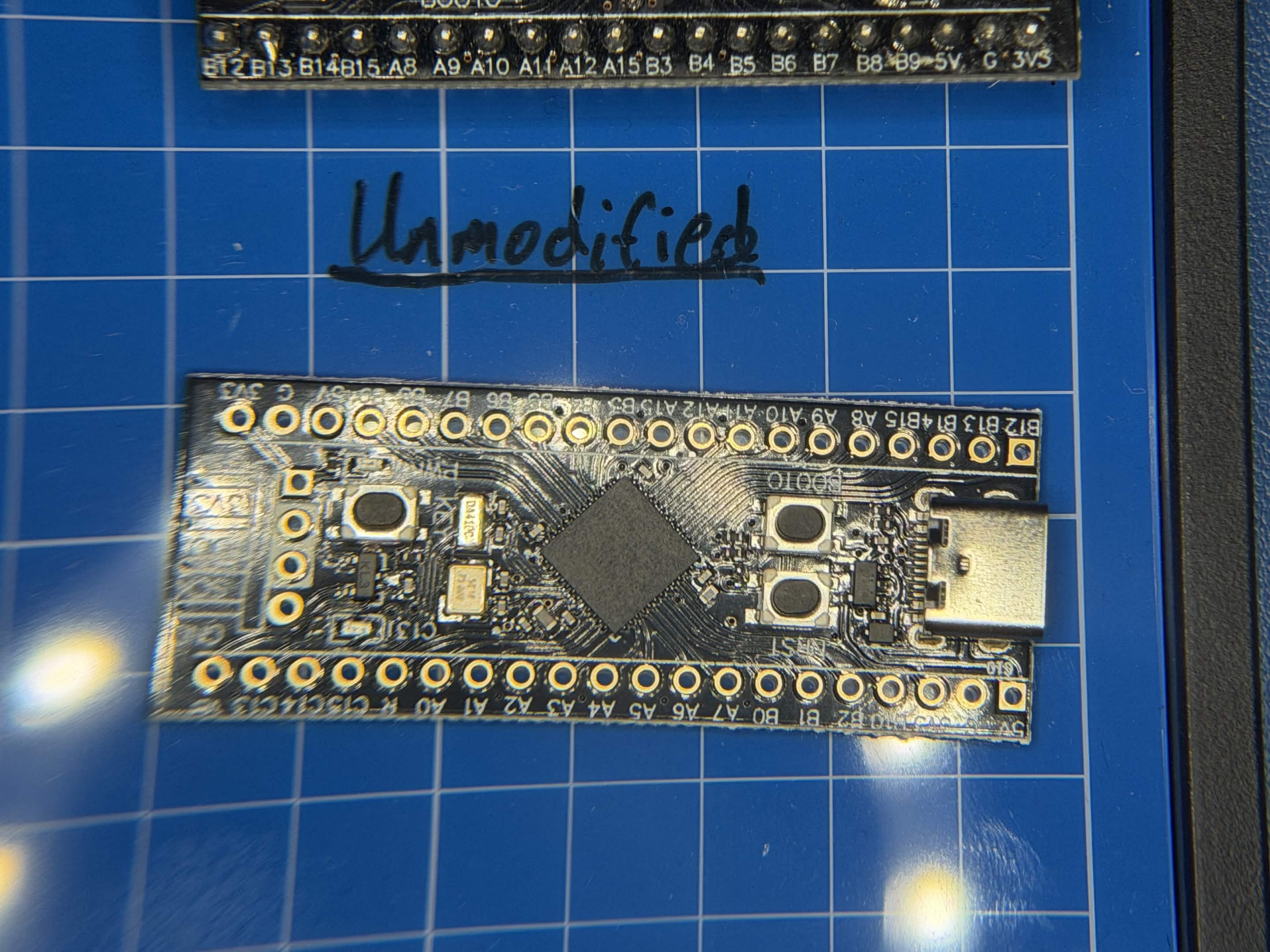
WeAct boards are relatively simple development boards, with support for a large variety microcontrollers that target a range of applications. If you’re situation is “I’m looking for a cheap development board that has this specific microcontroller”, then I wouldn’t feel guilty recommending you WeAct boards in general. They are available on amazon as well as most electronics sites for less than $4 and are simple in design with schematics of their power domain publicly available (here’s our target). At the beginning of my journey, I of course bought many units and carefully destroyed them. Here’s a quick sample of the Blackpill graveyard (some of which are embarassing, but I was still experimenting):
- Cut VCAP trace, breadboard shunt resistor
- Did not work, physical distance in the shunt circuit should be kept as short as humanly possible.
- Did not work, physical distance in the shunt circuit should be kept as short as humanly possible.
- Cut VCAP trace, insert makeshift shunt on-board
- Does not account for voltage drop across chosen resistor value and effects on expected operating supply to the chip. Likely board damage that is hard to avoid at this scale.
- Does not account for voltage drop across chosen resistor value and effects on expected operating supply to the chip. Likely board damage that is hard to avoid at this scale.
There are probably more than this, but I took a couple months hiatus from this project so my memory is fuzzy. The general lesson I learned is that generally, there is more to a setup that is required beyond inserting a shunt resistor on a random VCC pin (at least for a very great demographic of targets). And of course, this had to be where the randomness ends, because trying random stuff is stupid.
Eventually, I found this post on newae’s forum that looked similar to the situation I was dealing with (the traces from OP especially looked similar to the traces captured from setup #2) and I was able to note the following information relevant to my scenario. 1. My chip has an internal regulator which (at the time I thought) is likely significantly effecting SNR preventing all leakage, though of course that would not be the only factor. 2. While some variants of my chip feature a BYPASS_REG pin to disable the internal regulator directly, the package on the Blackpill does not support external power supplys. Of course, there are other ways to provide your own PSU and disable the internal regulator which we will talk about in-depth and which you can find more info on here: NewAE Targets with Internal Regulators.
VCORE When Possible
In most classic setups you might see someone lifting one of multiple VCC legs on an ATMega chip or Arduino-based devboard and shimming a shunt resistor directly off the leg. This does work and gets the job done perfectly for both power analysis and fault injection on basic microcontrollers. However for modern, complicated targets, there are a few issues to consider when you find yourself in this situation.
- If a chip has multiple VCC pins on the same domain sharing a power rail, putting a shunt on one of them might not catch all signal unless you find a VCC chokepoint for the power network which is easier said then done. Inserting a shunt on one leg might still allow current to flow freely and bypass your shunt through unshunted VCC pins, which might provide less of a current draw than is possible and less noise.
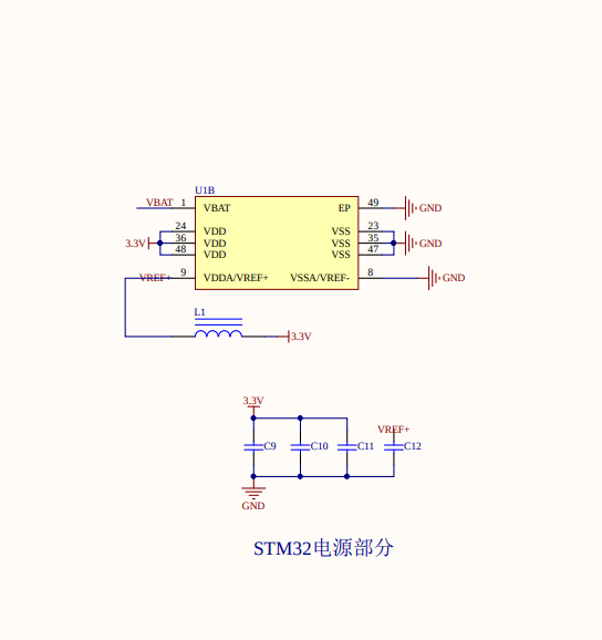 Power domain from Blackpill schematic. Notice the decoupling capacitors for all VDD pins.
 - VCC provides power to peripherals you don’t care about. This is not an issue specifically to VCC, but to pins in general that don’t route directly to a header. The farther you insert your shunt from the pin, more peripheral noise from the rest of the device’s components is introduced that you don’t care about. We only care about reading core voltage and not about stuff like I/O, LEDs, USB, UART, etc. This is easy to avoid when you have a package that allows you to pull a physical leg up and tie a shunt, but for packages like ours (UFQFPN48, solder joint), this becomes much harder because we have to choose a spot on the devboard. Furthermore, choosing a spot on the devboard becomes a greater engineering effort as we consider both this factor of peripheral current, and electrical concerns such as cutting a trace or soldering more small components than we have to.
Luckily, the majority of chips have another option of pin we can measure. Most chips run I/O and other peripherals at 3V3, but the internal core logic uses 1.2V or lower. To be a bit bold, almost every real mainstream embedded target you’ll encounter in your hardware research is going do this. This means while you may power your board with 3V3, there is an LDO within the silicon that brings the supplied voltage down to the regulated operating specification of the core logic.
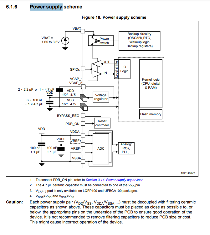 Power supply scheme for our target from the datasheet. Notice how all voltage supply besides flash access passes through the internal regulator before accessing core logic. Notice how there is also a BYPASS_REG that feeds into the regulator, which is not available on our package.
Wouldn’t it be better to target the core logic domain directly? Luckily for us, chips that feature internal regulators directly provide a feed. Even though the regulator is on-chip, its output needs external capacitance for stability and to respond to load variations. This provides a feed that is (mostly) our friend and a capacitor that (certainly) is our enemy. You will see this pin labelled names like VCAP (our target), VCORE, VDDCORE, VREG, and many others depending on vendor and chip. Note how on NewAE’s Details for their STM32F based UFO target when VCAP is present on an ST chip it serves as “the output of the regulator and input to the internal core logic”. These internal regulator pins are perfect targets, as they are singular, identifiable, outputs of VCORE.
RTFM: Setup OSINT
“OSINT is the epiphany of true pwn” - rondo
This is the most important section which I’m sure is unsurprising. When you are researching your specific targets here are a few sections from your target chip’s datasheet you will likely absolutely need information from:
- Power Supply / Power Management / Power Supply Scheme
- Describes your VCC feed, how it interacts with the internal regulator if present, and so on. Describes what modes exists, pins connected to the VCC network, and if any bypass exists.
- Operating Conditions
- Contains the internal voltage for your regulator. This will come in useful when we try to bypass it and help us know the safe maximum voltages we can safely apply externally on the pin (explained later).
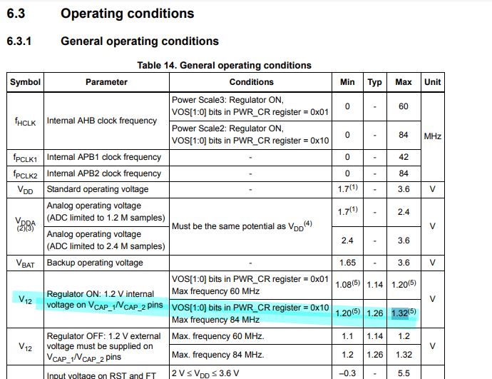 VCORE has an internal 1.2V domain
- Contains the internal voltage for your regulator. This will come in useful when we try to bypass it and help us know the safe maximum voltages we can safely apply externally on the pin (explained later).
- Pinout
- I always love to use this to label a screenshot of my actual taget with VCC and VCORE pins.
- Block Diagram
- Helps illustrate interaction between VCC, internal voltage domain, and remainder of internal core.

- Helps illustrate interaction between VCC, internal voltage domain, and remainder of internal core.
- External Capacitors
- Tells you what capacitor values are used to stabilize the regulator and how to account for changes in the circuit.
 Note how for our target, a single 100nF bypass cap should be used when providing an external supply.
- Tells you what capacitor values are used to stabilize the regulator and how to account for changes in the circuit.
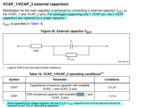
In finding this information, we have found most of the details we will need to build our measurement circuit. There is of course additional information you’re likely to find not mentioned here that will prove extremely useful to your setup, and I will mention some of the specifics for the STM32F401xC later. It is at this point I recommend you label a picture of your actual target pinout for your own sanity (trust). You can find pin 1 by identifying the dot and verify your VCC pins as well as the decoupling capacitors connected to them by using your DMM in continuity mode. Keep in mind the decoupling capacitors for VCAP and VDD will be found as physically close to the pin as possible to provide the best noise reduction. 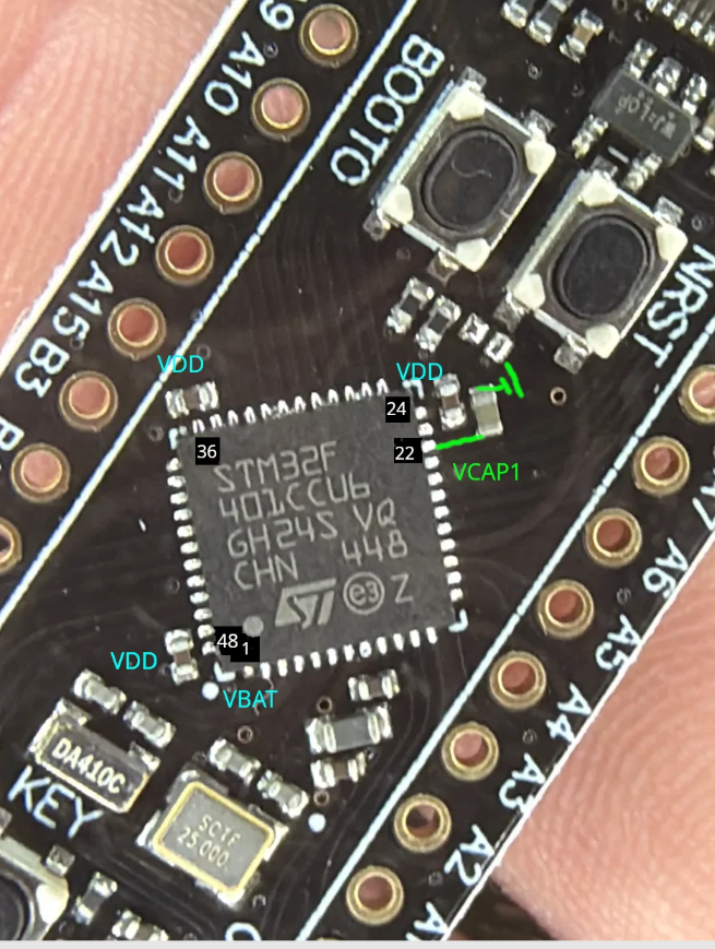 My labeled overly neat pinout, that I will be referencing from here on.
High-side and Low-side
The classic SCA setup is to take a high-side measurement on VCC, that is: PSU -> shunt -> VCC. In this scenario, you would measure the voltage drop on the 3V3 supply rail. In our approach we will be taking a low-side measurement on VCAP, that is: PSU -> shunt -> VCAP -> GND, the difference here being we measure the voltage drop across the signal from the regulator itself. This way, we are directly on the core domain instead of a domain mixed with I/O and other current that flows through VCC. Recall that VCAP serves as an output of the internal core logic. This is the main difference. More generally, high-side refers to the circuit between the positive supply and the target while low-side refers to the circuit between the target and ground. VCAP is tied to ground so this is a low-side measurement. From here on when designing our capture circuit I will be refering to placements in terms of the high side (HS) and low side (LS) of the VCAP node (that is after and before our shunt).
SNR and Capacitors
You’ll be dealing with capacitors frequently when developing your more advanced measurement setups, both in removing decoupling capacitors and possibly adding your own bypass capacitors. Note that for any voltage pin you’re measuring, be that VCC or VCAP, decoupling capacitors will make your signal-to-noise ratio much worse (as is their purpose). You will quickly learn that anything beneficial for signal integrity and stability (such as the internal regulators themselves) are bad for power analysis. Components like this smooth out voltage variations that would otherwise occur due to CPU computations that we are interested in measuring. They create stable feedback loops for the domains they are connected to, but much less impressive differences in traces for us to measure. We want the signal to be electrically “raw” and as unfiltered as possible. So it is almost always recommended to remove the decoupling capacitor(s) connected to your target.
You can identify if a capacitor is a decoupling capacitor for your target pin with a simple continuity test. One side of the suspected decap should be connected to your target pin and the other side should be connected to ground. Here we have identified the VCAP decap here. 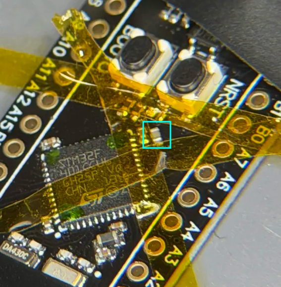
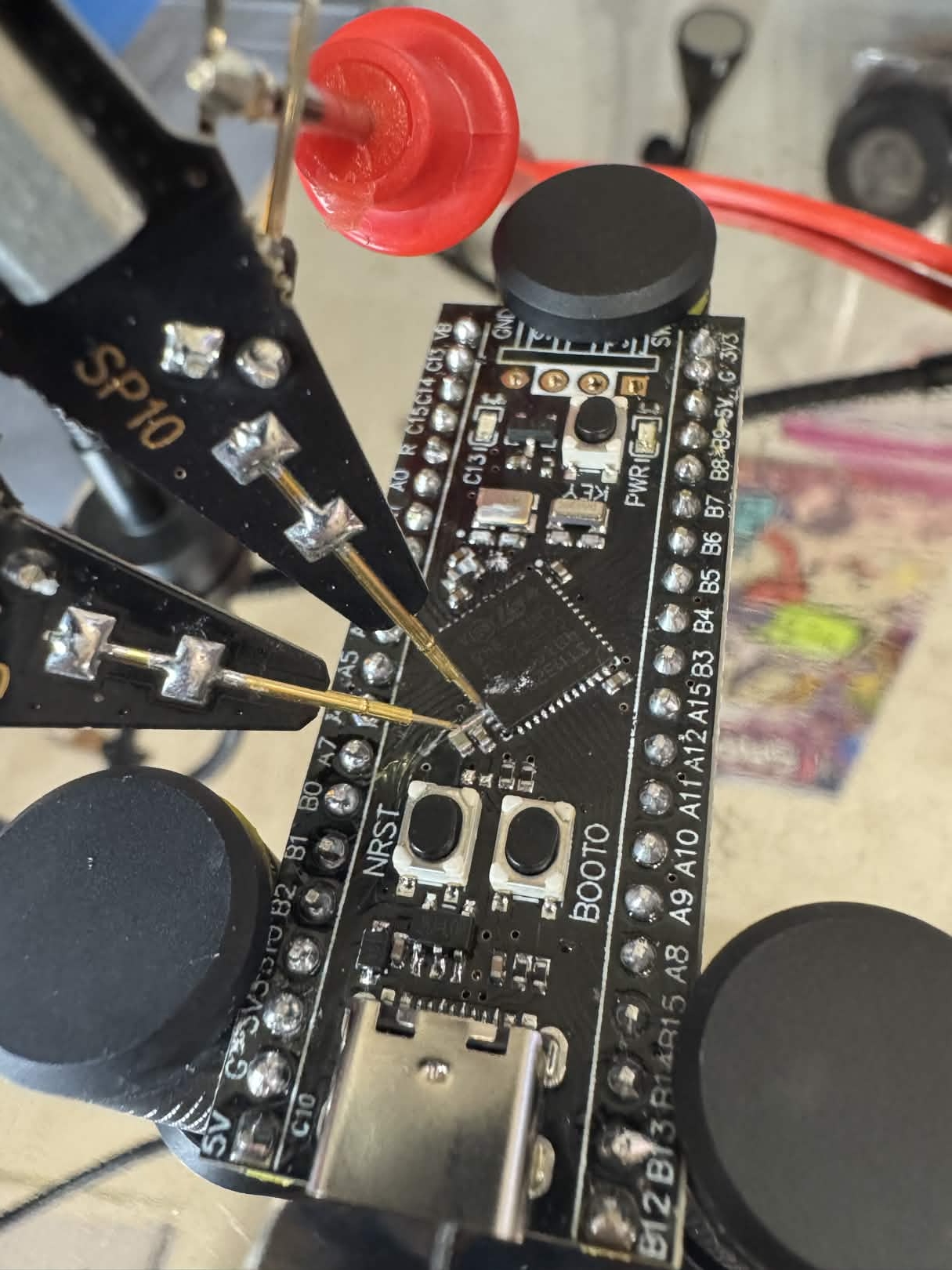
Removing this will not only provide much better SNR, but will also provide a pad we can solder to that lies on a clean and open trace directly to VCAP with no other components on it and far away enough from the chip so as not to damage it with our shenanigans. This is useful because it will disconnect VCAP from ground, allowing us to solder a connection from this pad to a short circuit off-board. This circuit will include our shunt measurement and other components we’ll shortly cover. Remove your decoupling capacitor(s) using a heat gun or a soldering iron and tweezers. It is recommended to apply heat tape to protect surrounding electrical components. Be sure to also constantly clean up your board with flux remover solution if you keep applying bloches to avoid accidental bridges from here on.
Also recall that the datasheet noted that when the internal regulator is not being used, we should be supplying two 100nF bypass capacitors to our external power supply if VCAP_2 exists. This external supply is not a part of our measurement and we’d like it to be stable and safe from EMI, so we will be adding a single 100nF bypass capacitor to our circuit right off the PSU.
Internal Regulators and Defeating Them
We already know quite a bit about our target’s internal voltage regulator. We also know that we’d like to perform a VCAP node measurement to reflect only core logic. But we also should note that internal regulators themselves are detrimental for power analysis. They actively suppress and flatten the signal we are trying to measure to a specific operating voltage. The job of the LDO is to maintain a constant output voltage regardless of changes. This means if the CPU consumes more current because of a computation we aim to measure, the LDO responds to keep the voltage as stable as possible. It stops us from observing current variations directly or significantly reduces the noise produced from these variations. So how do we deal with them? This sounds like a situation similar to the decoupling capacitor, except unlike the decap we can’t interact directly with the LDO (at least not without red-fuming nitric acid). Luckily for us both our datasheet and NewAE make our path forward quite clear.
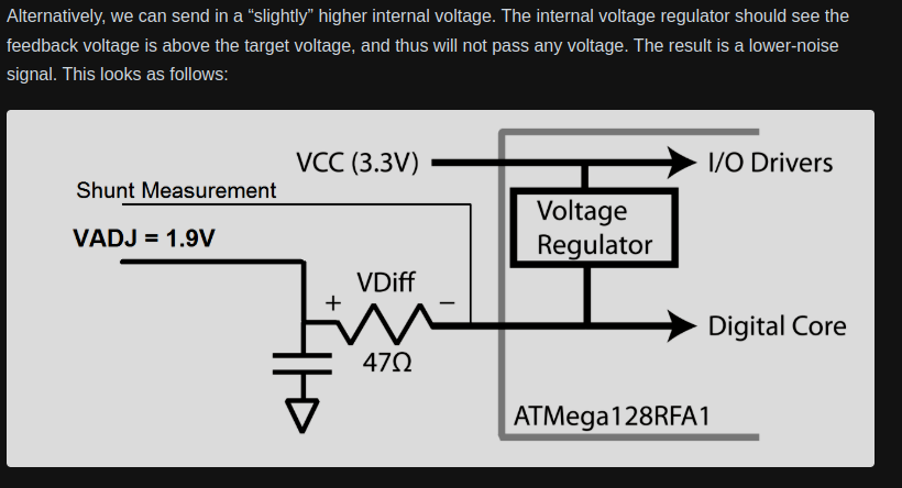 Perhaps the most useful diagram in this post: https://chipwhisperer.readthedocs.io/en/latest/cw_tips_tricks/advanced_usage/regulators.html
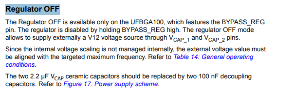 The factory, regulator off, BYPASS_REG is not present on our target, but the datasheet specifies we can supply voltage through the VCAP pins. It also confirms the external voltage supplied is not scaled to the internal expected operating voltage of the LDO and that we should do that, so naturally we won’t.
This confirms that if we provide a slightly higher voltage to the VCAP output, the regulator will not operate since it is being fed a voltage higher than it is capable of regulating. How do we find this perfect voltage without permanently damaging the chip? I’ll go over this in a simple method called “regulator sweeping” which is a name I’ve just made up, just now. I am sure it has however, been done a thousand times. We now have a way to turn the regulator off and have enough information to start drafting (and I recommend you to draft first) a measurement circuit. The most important part is the VCAP pad where the 2.2uf decoupling capacitor used to be. It will be responsible for the following:
- High side: PSU -> 100nf bypass -> Shunt
- Low side: Shunt -> CW Measure -> VCAP
In this regard, this point on the devboard is responsible for the low side measurement, disabling the regulator via external supply, and ground.
Circuit Design
Before we design the measurement circuit, here are some quick tips we didn’t use here, but will prove useful to know:
- Check if NewAE has a UFO adapter for your target chip. This can help you design a circuit based on theirs. Note one exists STM32Fx and it appears they also target VCAP.
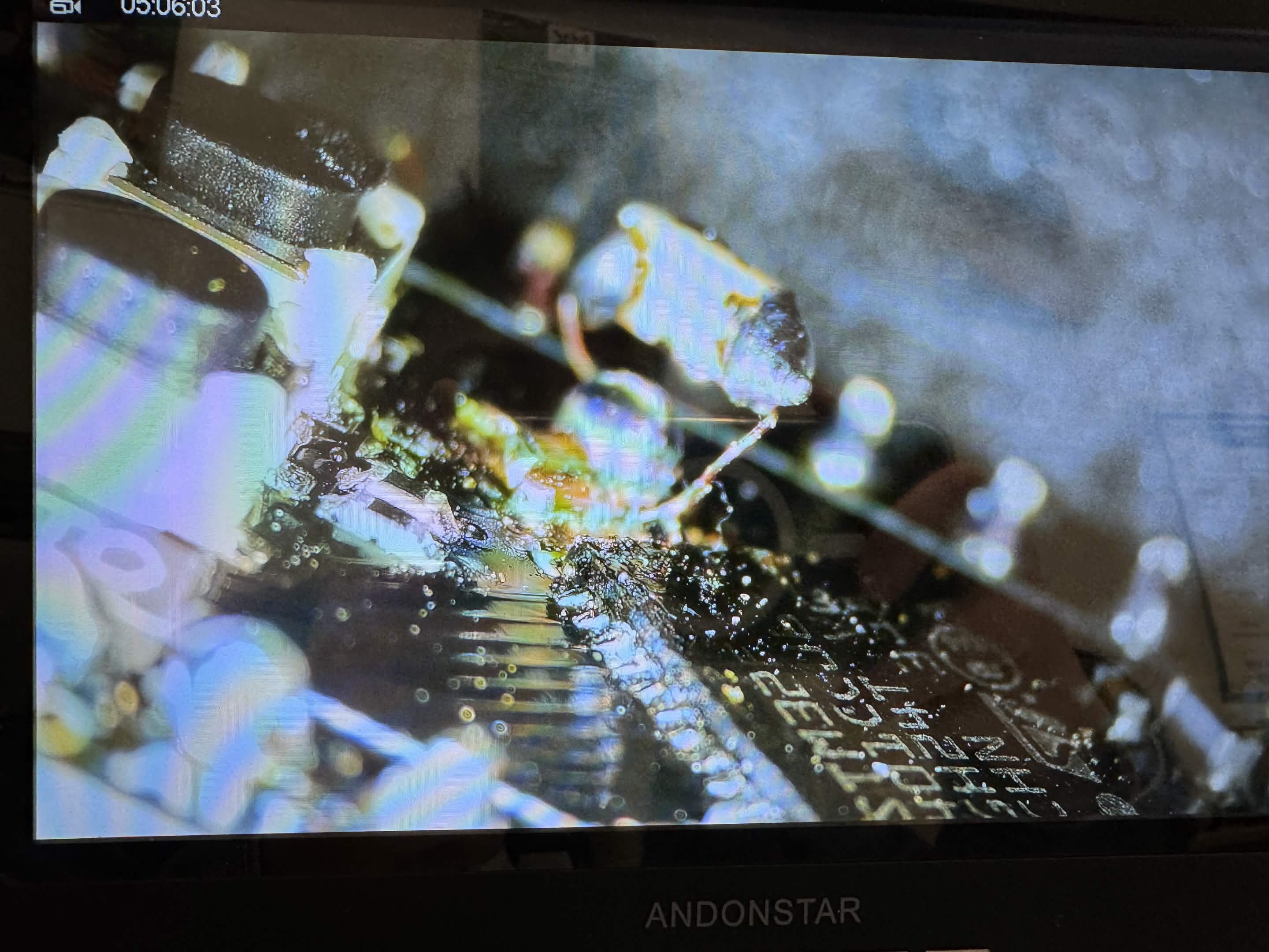
- If your devboard is open source, or has anything such as step files online, you can verify where specific components are. Here I am verifying the decoupling capacitor I already verified electrically is connected to VCAP using a step file from the github repo.
 Verify visually that C8 is the VCAP decap. https://github.com/WeActStudio/WeActStudio.MiniSTM32F4x1
I recommend you flash your target with the firmware you want to perform the attack on (unless you’ll be doing that using the 20-pin header) now. Also please do note that physically, we want the circuit to be as small as possible as to eliminate EMI, especially the connection that will be going from the VCAP pad and onto our external circuit as this will be the most sensitive and important. We will be implementing our own circuit on a protoboard that is connected to our newly exposed VCAP pad. Use a thin gauge wire for this connection, I ended up pulling a single copper strand from a jumper, and soldering it carefuly to the pad (remember the pad connected to VCAP, not ground) before building the actual circuit it will connect to.  If flux was applied, remember to apply remover solution to avoid bridging VCAP to the ground pad. Verify with your DMM this is not the case.
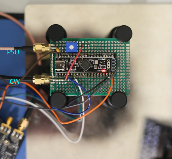
Next I prefer to add connections on the protoboard for the actual chipwhisperer 20-pin header before actually building the measurement circuit. For my setup, I ended up doing the following:
- Blackpill 3V3 -> CW 3V3
- Blackpill GND -> CW GND
- Blackpill A8 (Added clock output) -> CW HS1
- Blackpill B0 (Trigger) ->CW TIO4
- Blackpill R -> CW nRST
- Blackpill A9 (TX) -> TIO1
- Blackpill A10 (RX) -> TIO2
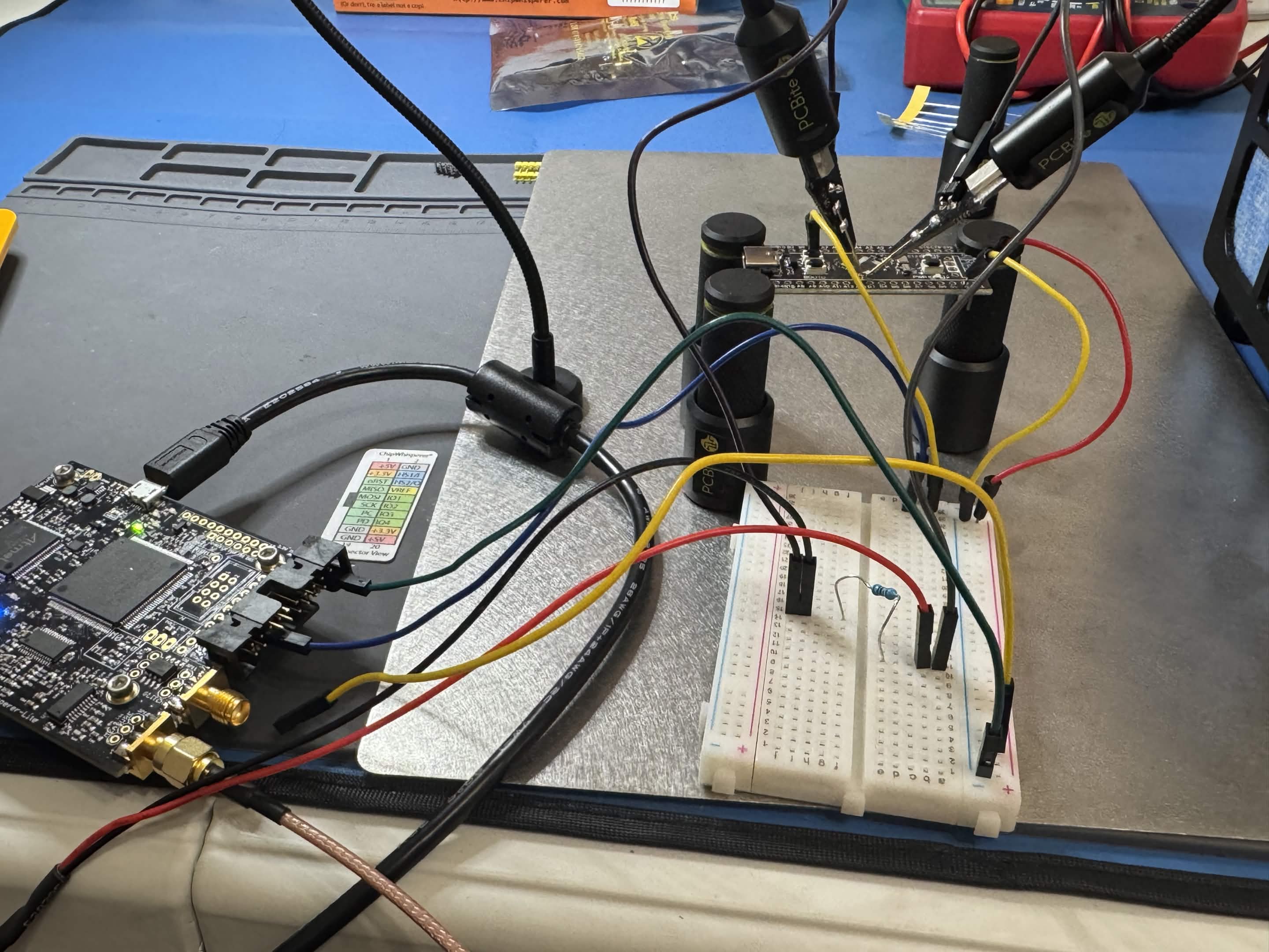
Next we can implement the measurement circuit. Remember we want to design this with minimal physical distance on the high side and low side of the shunt resistor. A couple subtle tips:
- My perfboard does not have connected rails. If this is the case for you, you can place single copper strands to create solder bridges (bridges won’t hold over the perfboard silk no matter how big you make them, trust me).
- Use an SMA connector and coax cable for the measurement signal to the chipwhisperer, again to prevent EMI. This does not matter as much for the power supply line, but I did so here as well.
- Measure out the path on your perfboard ahead of time so as to use the minimum amount of holes for your components and therefore minimal distance.
- Trying to thread the VCAP strand through a thru-hole risks tearing it off the pad. Tape it against your hole and solder over it. Remove tape and cut the excess wire with an exacto knife or scalpal.
- All grounds must be shared with the chipwhisperer to prevent ground loops. Your entire measurement circuit should share a ground with your chipwhisperer, the CW will take measurements relative to its own ground. The PSU and blackpill should both have a path to chipwhisperer GND.
Do note the PSU is being used to override the regulator, not power the 3V3 rail. This should be done by the chipwhisperer or another power source. I also prefer using a trimpot instead of a plain resistor for the shunt measurement and I am not sure why it isn’t talked about more. Later in regulator sweeping you will see that we are going to be looking for a magic resistance value that offers the highest manageable resistance value, while not causing so much of a voltage drop that the internal regulator turns back on. A trimpot is useful here because you can continuously tune the resistance value via the wiper, without having to keep resoldering resistors.
In general the measurement circuit looks like this: PSU -> 100nf Bypass -> Shunt Trimpot -> CW Measure -> Removed decap -> VCAP.
The circuit itself was much inspired by this extremely helpful blog post from Bedri Zija Breaking Hardware AES on the MSPM0G3507: From Zero to Key. Luckily, enough his target was also a Blackpill board and he posted this near the end of my research which allowed me to make corrections to my capture setup using his setup picture. He also gave me the trimpot idea. Here is a general schematic of my setup for the STM32F401xCC (generated with Claude by giving it the pin connections): 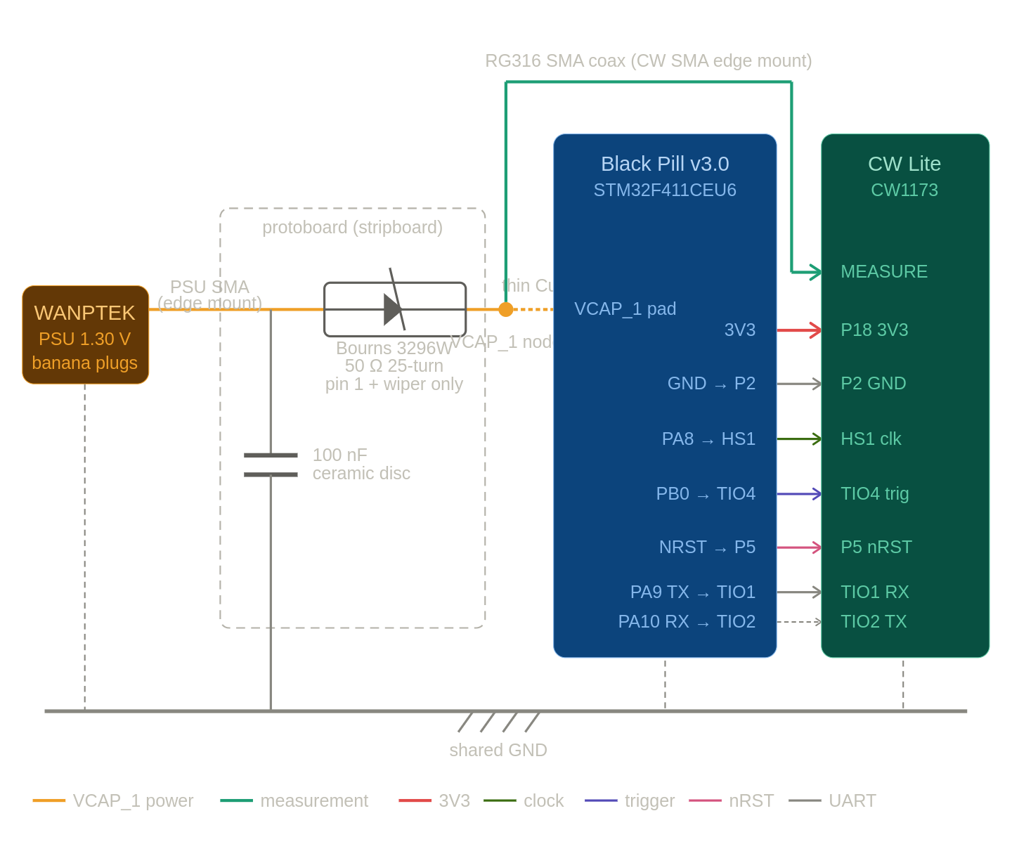
Verification
Verify your circuit works electrically before continuing.
Continuity Tests:
- PSU GND -> CW GND
- CW SMA -> CW GND
- 100nf LS -> CW GND
- 100nf HS -> CW Measure
- Blackpill GND -> CW GND
- Blackpill VCAP -> CW Measure
- Blackpill VCAP -> PSU
- Ensure PSU and Measure are open to the ground strip, if they aren’t, you have a short you need to start looking for.
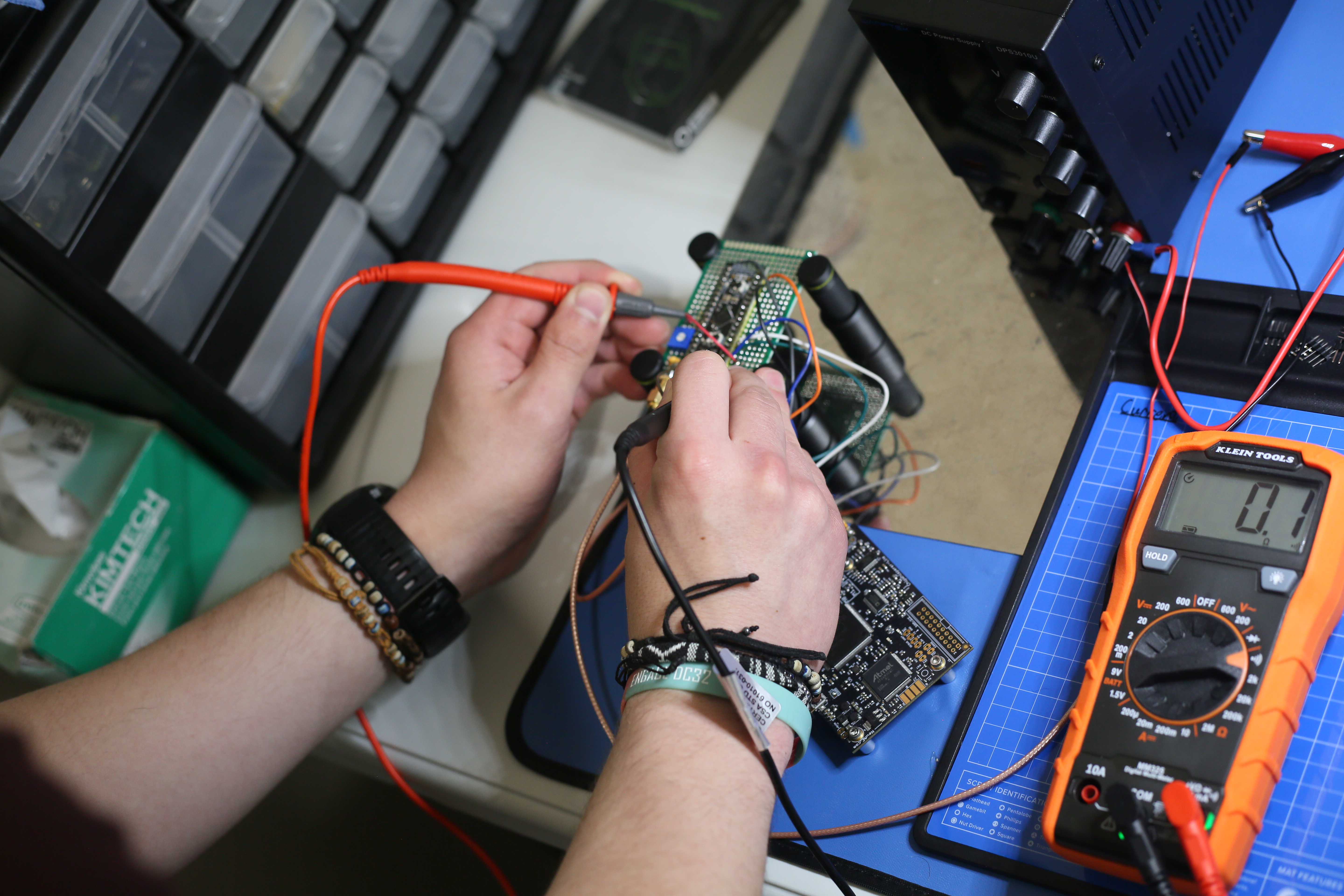
Measurement signal path and shunt resistance: DMM in resistance mode, probe PSU and CW Measure. You should read the resistance value, which you can change on your trimpot.
Verify firmware without external PSU: Ensure PSU is physically not connected, then power with your chipwhisperer (or USB) and confirm your 20-pin connections still work with your firmware. Here is the jupyter notebook I wrote specifically for this target.
Final circuit:
 Note: don’t test with the PSU yet.
Verification is important. A short between VCORE and ground will result in your chip likely being permanently damaged when external power is supplied. Please also double check both legs of any capacitor as mentioned above.
Regulator Sweeping
The process of iteratively testing values during the characterization phase (finding the right set of values that build our model) is known as “sweeping”. This “regulator sweeping” is no different in its purpose. Here we are characterizing two component values:
- The PSU load
- The resistance value of the trimpot
Set the PSU too low, and the internal regulator remains on. Set it too high and you will likely destroy the chip. We also want to find a resistance value that lets enough of the PSU current through so as to not only keep the target chip operating, but to keep it operating with its LDO off, and furthermore, still be big enough so that we have clean traces. The larger the resistance value, the larger the voltage drop, and therefore, the greater liklihood that the voltage won’t turn off the regulator (even though the PSU voltage is well beyond specified operating conditions).
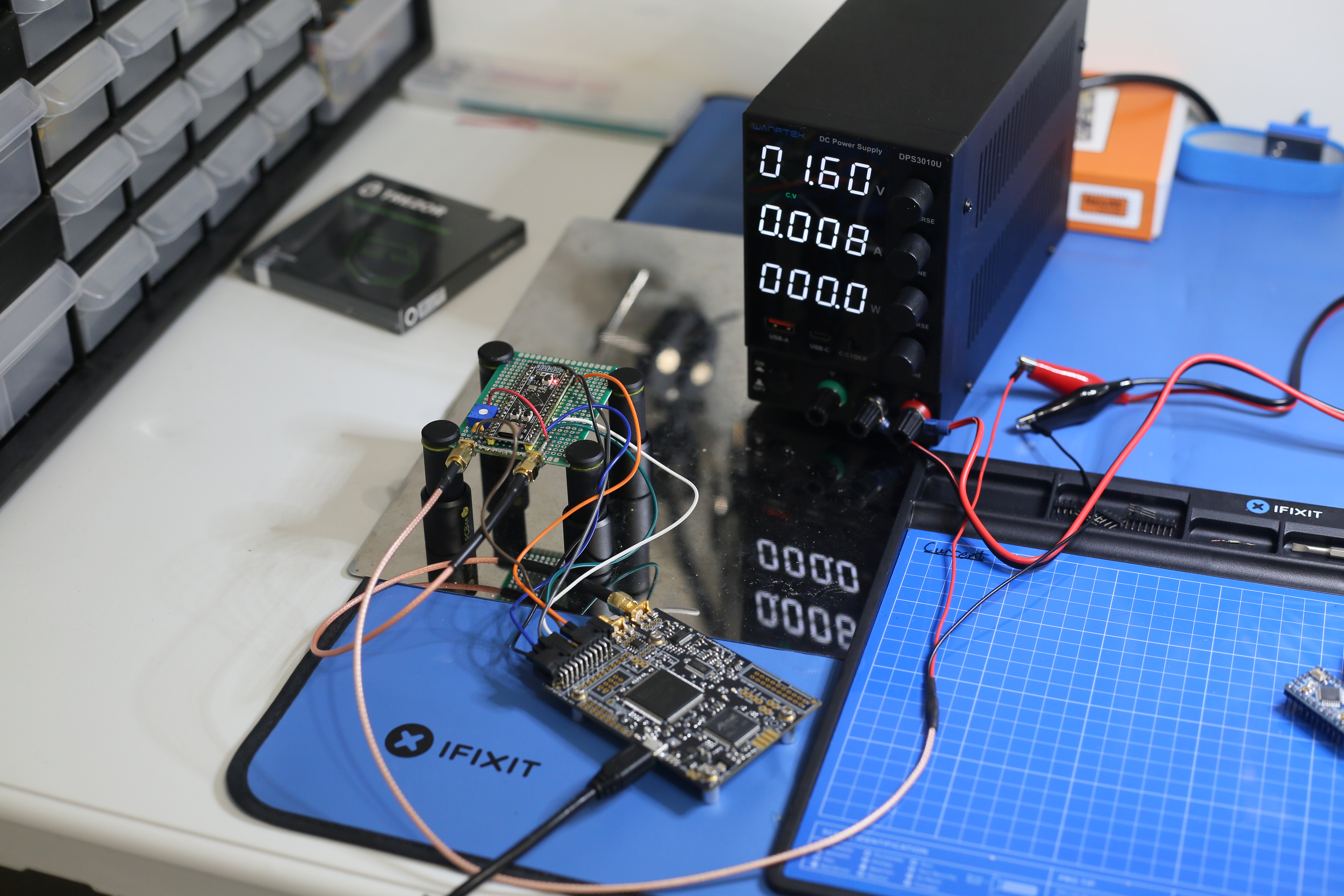
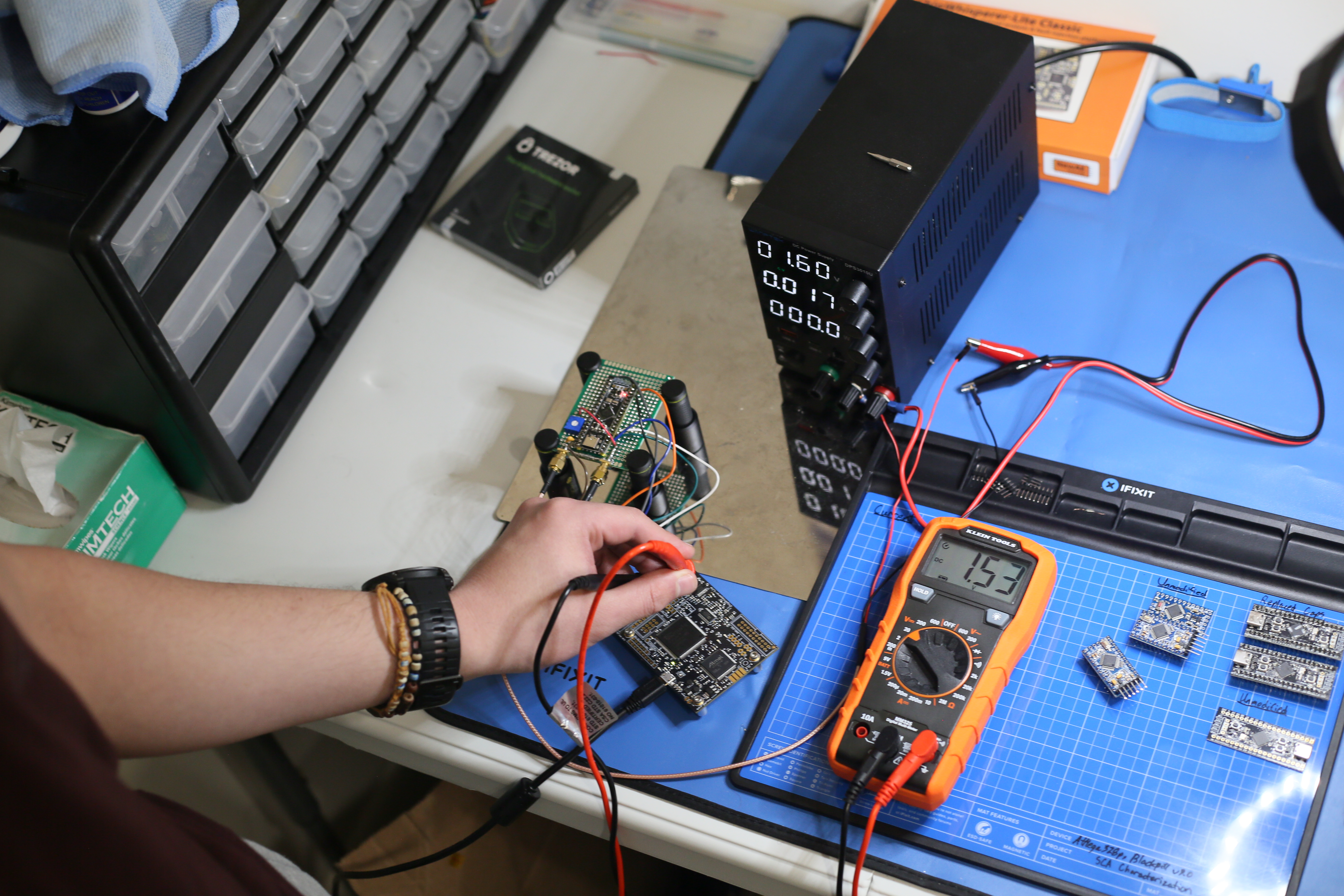
I recommend you start by disconnecting the PSU and powering the target. Measure between GND and CW Measure with your DMM in voltage mode. You should read a value close to the specified internal domain voltage from the datasheet. 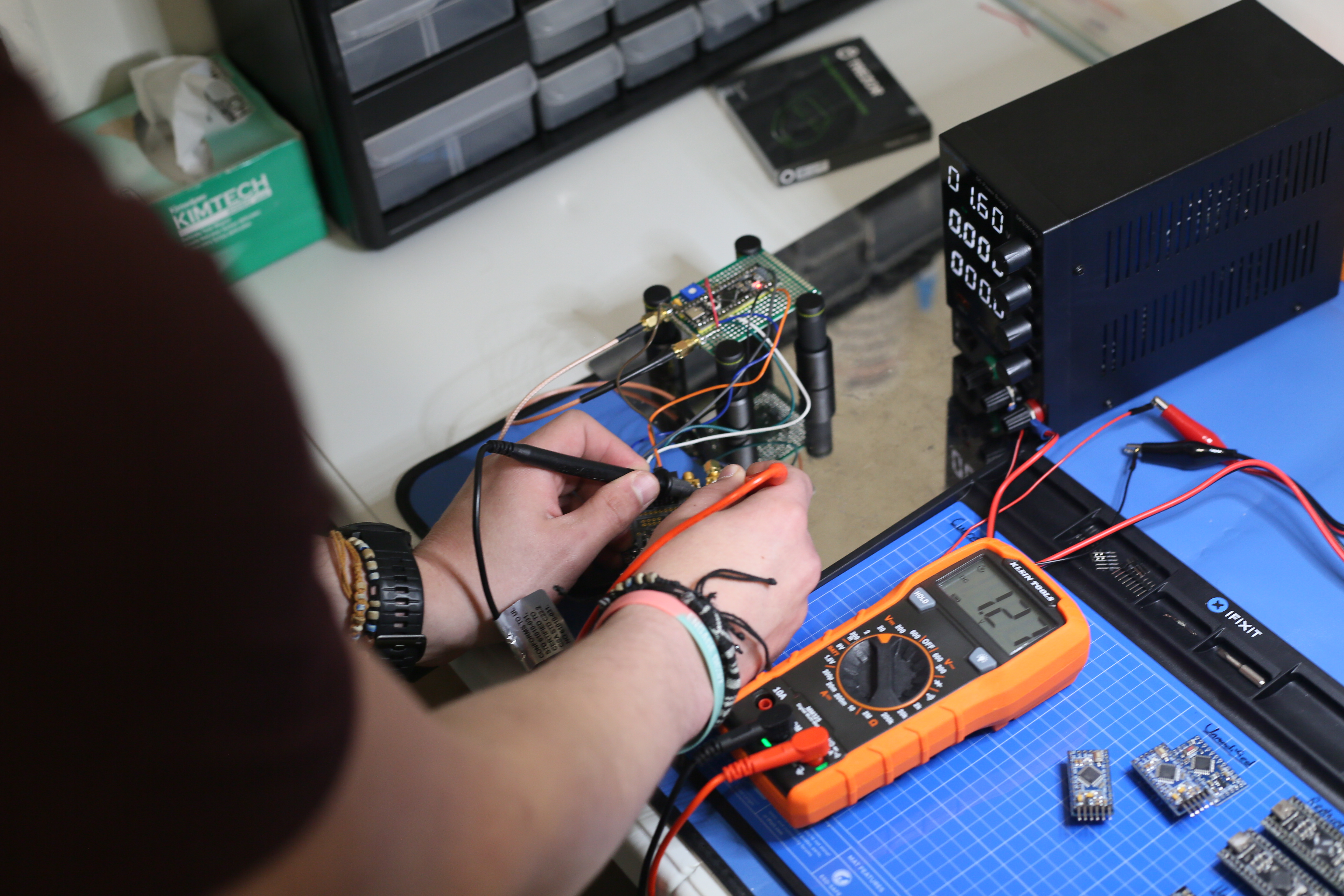 The PSU is on in this picture, but the trimpot resistance is so high the LDO didn’t turn off.
Start with your trimpot on the minimum resistance and turn on your PSU. Start with a supply voltage that is slightly over recommended. I originally started with 1.3V. Notice how the target is a 1.2V domain, with its maximum at 1.32V, which this is still under. Start small. Take the voltage measurement with your chipwhisperer and increase the PSU voltage coarsely, until the DMM no longer reads the regulator voltage, but a drop off variation of your external supply voltage. 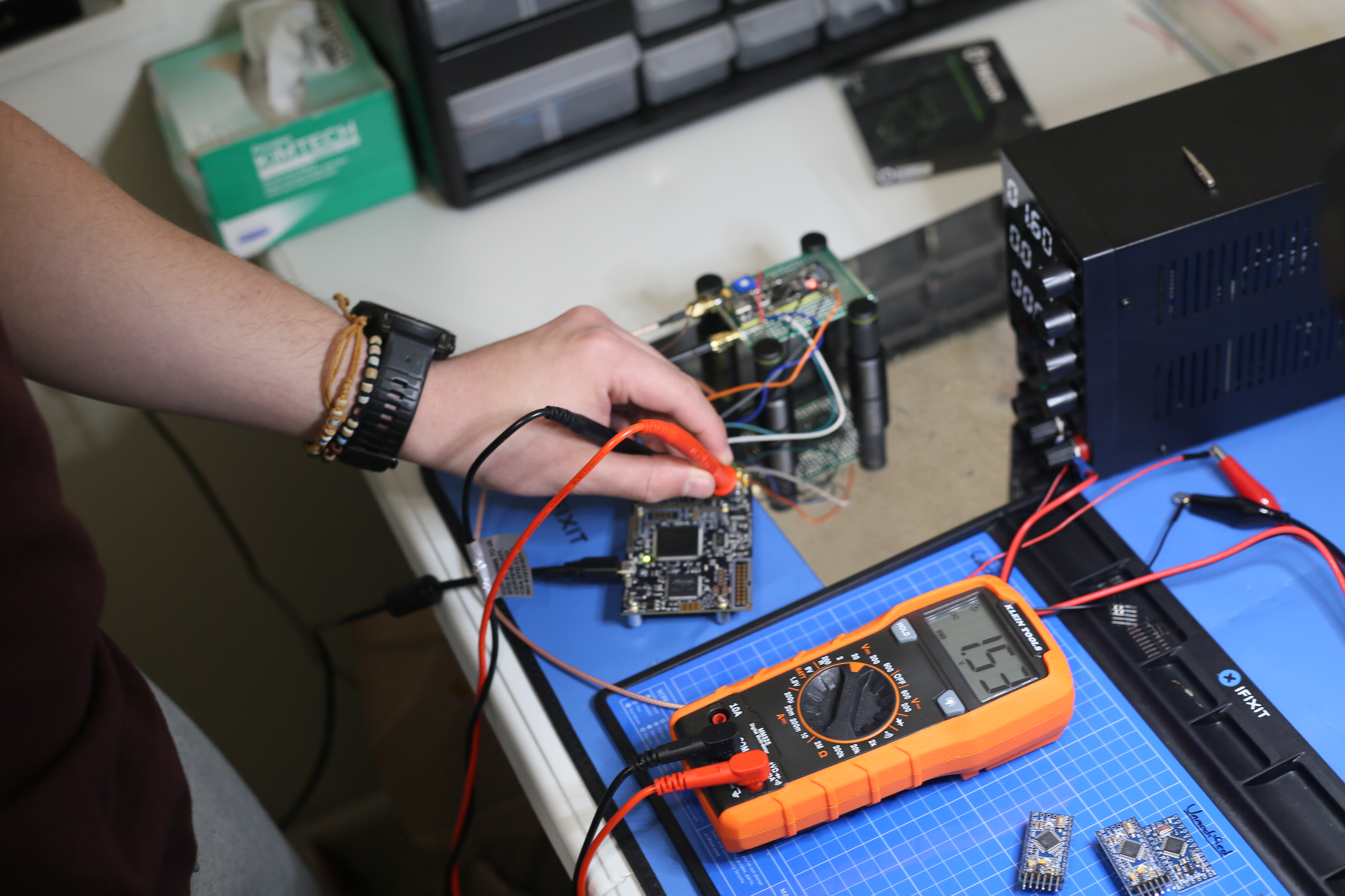 PSU=1.60V, Signal=1.53V, clear the internal regulator is off.
Continue increasing your trimpot to the desired resistor value and performing this test again until you reach an LDO turn off with the desired resistance value. A higher resistance will produce a stronger signal. Do note that the goal is not to get a high reading on your DMM. As long as the voltage is even slightly higher than the specified operating voltage the regulator has been turned off. After this process, you should have your final circuit and the perfect external supply voltage and resistance values.
Power Analysis and Window Tuning
Congratulations. This post was meant to serve as a general guide on taking measurements of any external and non-target designed board using your chipwhisperer. We finished that part. You can now continue with your relevant attack goals. If you have any further issues with SNR, check that all decoupling capacitors for your specific domain were removed and the appropriate bypass capacitor is provided to your power supply. The remainder of this post will talk about my target specifically. My jupyter notebook has the following code blobs designed to leak SPA firmware from the STM32F401xC:
- Verification firmware works
- Verification trigger signal is being spotted
- Verification we are able to RST the Blackpill
It is then followed by scope configuration where the number of samples and offset from trigger before capturing is defined along with the target clock. Here we use “extclk_x1”, which will sync the scope with the clock signal we have on HS1. I then have 4 capture tests. Note the firmware password is testpass.
- Repeat captures: The traces should nearly line up.
- Partial to complete password: The traces should spike away from the correct password trace and into the general loop depending which position the first incorrect character occurs.
- Visual trace outlier for first character (“t” should be the outlier).
- Print SAD for every possible first character (“t” should be highest).
- Basic SPA Attack (requires good SNR)
- SAD SPA Attack (requires okay SNR)
The goal of this post is not to go over basic power analysis concepts, but instead the actual hardware setup that is frequently not covered. For that reason this section of the post will be relatively short and aim only to prove that we have successfully leaked the password from the Blackpill STM32F401xC firmware using this setup. The success of this attack depends on your physical capture setup. I recommend you first narrow your capture window before trying the SAD variation of the attack. To do this, keep the defaults and take a capture with a completely incorrect password (the first character is any character besides “t” and the password is 8 characters long) and the correct password. Note the trace number where the traces start to drastically diverge. Note the trace number where they return to each other. This is your scope.adc.offset and scope.adc.samples respectively (samples is actually the full capture window, but for SPA this is usually good enough). The finished attack here takes just over 200 traces for the 8-byte password (LDO off): 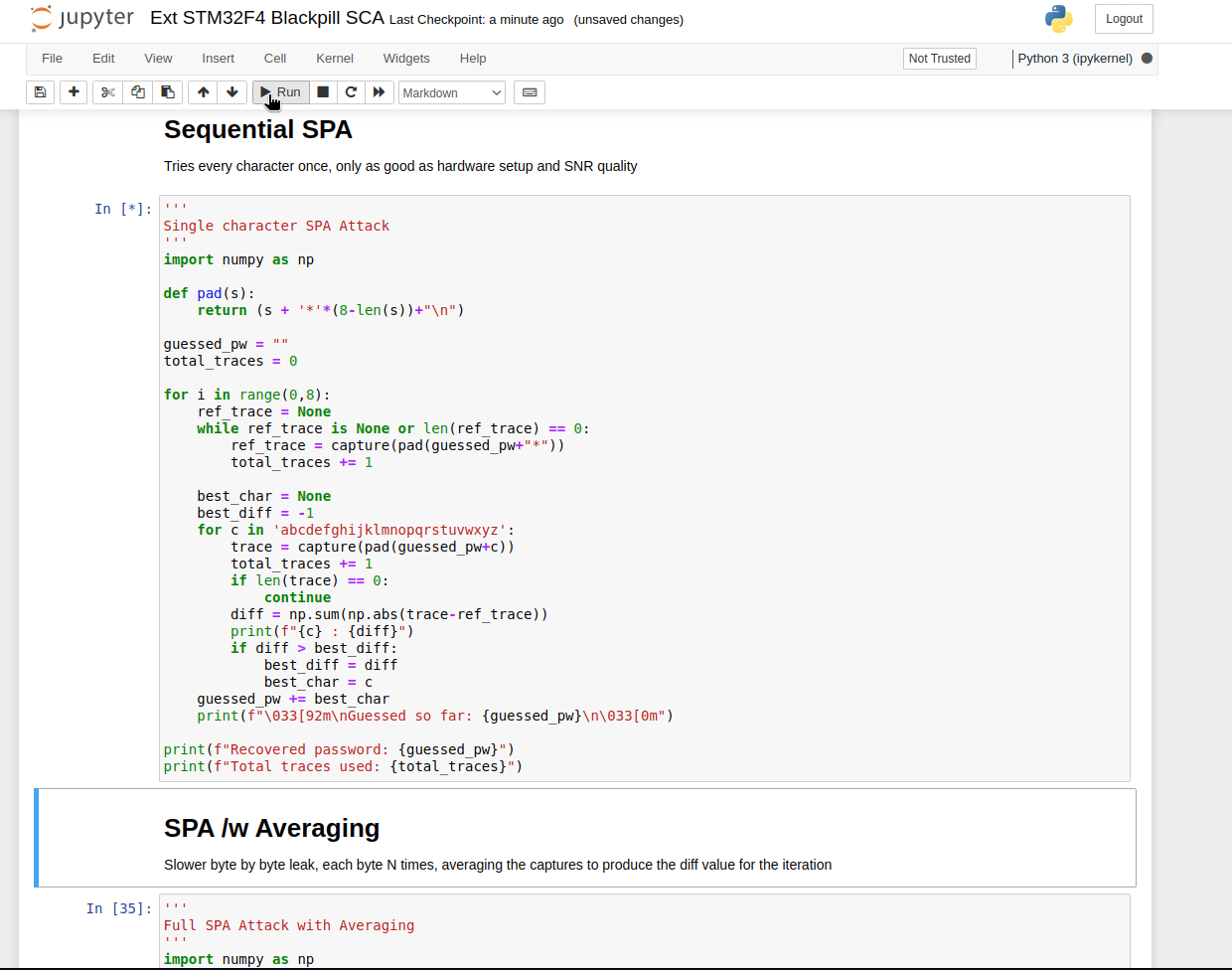
Formally Proving SNR is Better with the STM32F Regulator Off
A Note on the STM32F401xC’s LDO
The SPA attack provided here still works with the STM32F internal regulator activated. So why does SPA work with the regulator still on? Does SNR actually improve with the regulator off at all? Will this proof section make my professor finally proud of me? We’ll answer some of these questions definitively here. As it turns out, yes, for this specific target, there is enough noise that this attack works with the internal regulator still operating (at least for SPA). However, there does exist a significant SNR advantage with it off. I tried to prove this empirically with a simple experiment. Recall (or note) the following SNR definition:
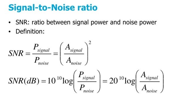 The first definition of SNR is all that is relevant.
The following is the experiment design I ran:
- Regulator on and regulator off control groups, each averages the results of the following over 10 iterations:
- Capture and average 20 reference traces
- Capture and average 20 traces for the current character
- Compute the SAD against averaged reference mean
This gives us the following values:
- SAD for t (tSAD): The absolute signal strength for correct character, “t”.
- Distance from “t” to minimum value
- SNR: Ratio of tSAD to mean noise across all incorrect characters combined.
SNR=tSAD/mean
This experiment produced the following results (rounded to 4th decimal place):
- Regulator overridden
- tSAD: 4.7281
- Dist(t->min): 4.3949
- SNR (tSAD/mean): 11.6542
- Regulator in-use
- tSAD: 5.6134
- Dist(t->min): 5.0178
- SNR (tSAD/mean): 7.7914
Let’s first note the SNR between the two groups. With the regulator override, the SNR is 11.6542, nearly 50% better than that with it in-use. I have no doubt that with larger control groups or more complicated models which require significantly more traces (CPA, DPA, Reverse Correlation, Template Verification, etc) that the difference is significantly greater and a factor that must be accounted for as opposed to SPA. Upon closer glance at the results we may question why the distance from the worst character to the correct character is shorter for the regulator overridden group. In theory, we’d expect the opposite, a larger distance would produce more obvious noise on the traces that would make it easier to tell if a character was correct or wrong. The only explanation I can offer is speculative, that being the regulator in-use group has an inflated tSAD and mean noise value. Specifically, the worst characters (min) in the regulator overridden group has a smaller value than that of the in-use group. This goes to show why simply measuring the diff of “t” alone would be too simple a metric. The only metric that is meaningful and that matters to us is the SNR after all, and the goal is to improve it via our capture setup in every possible way before improving our models.
Key Takeaways
- Target core logic domain directly if possible
- Almost every modern embedded target has an internal regulator with an exposed supply pin, which directly reflects core current and avoids irrelevant signal.
- Decoupling capacitor removal is twofold
- Eliminates signal smoothing and serves as a point of regulator control input if the target is the regulator.
- Datasheet defines your capture circuit
- Design before you implement. The datasheet tells you your core voltage domain, bypass capacitor values if needed, and decoupling capacitors near the chip. Searching specifically for the phrases listed in the OSINT section leads to useful results.
- Physics
- Physical distance kills SNR. The wire that connects your circuit to your target is the most sensitive connection in the setup. Use thin gauge. Shared ground isn’t optional. Verify your circuit electrically before powering, a short off of the VCAP node can damage the target chip if external power is applied. SNR is the only metric that matters for verification purposes.
- Internal regulators fight you
- Maintaining constant output voltage reduces SNR.
- Consider a trimpot shunt over a resistor to make verification and future shunt modification easier!
Future Research: While I haven’t seen anything public on this chip in regards to power analysis via regulator turn off, for future research I plan to target more under-researched and complex embedded appliance targets such as automotive chips. I was previously inspired to do more automotive research and now share this specific desire thanks to Bedri Zija.
Thanks for reading, I hope this guide proves useful!
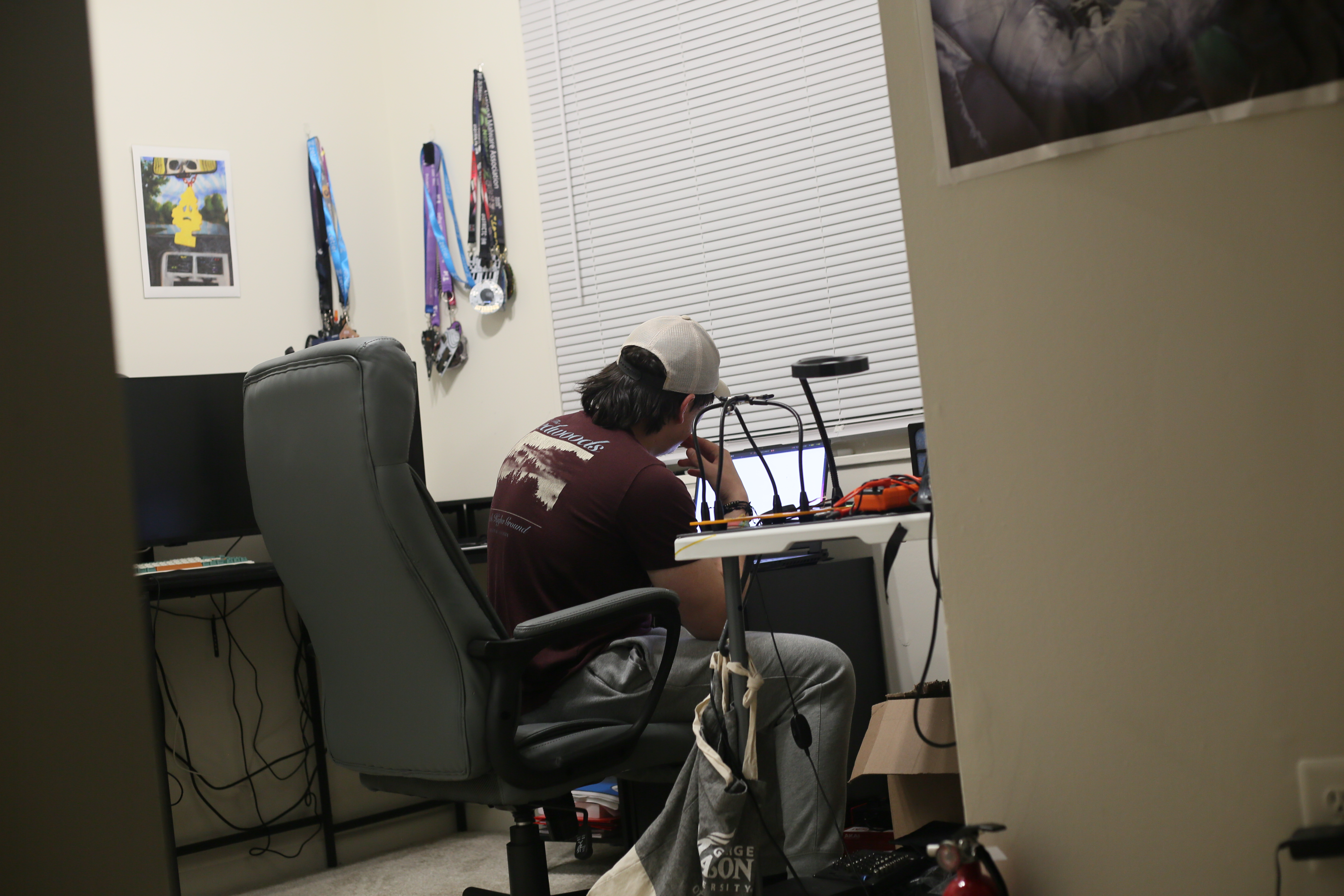
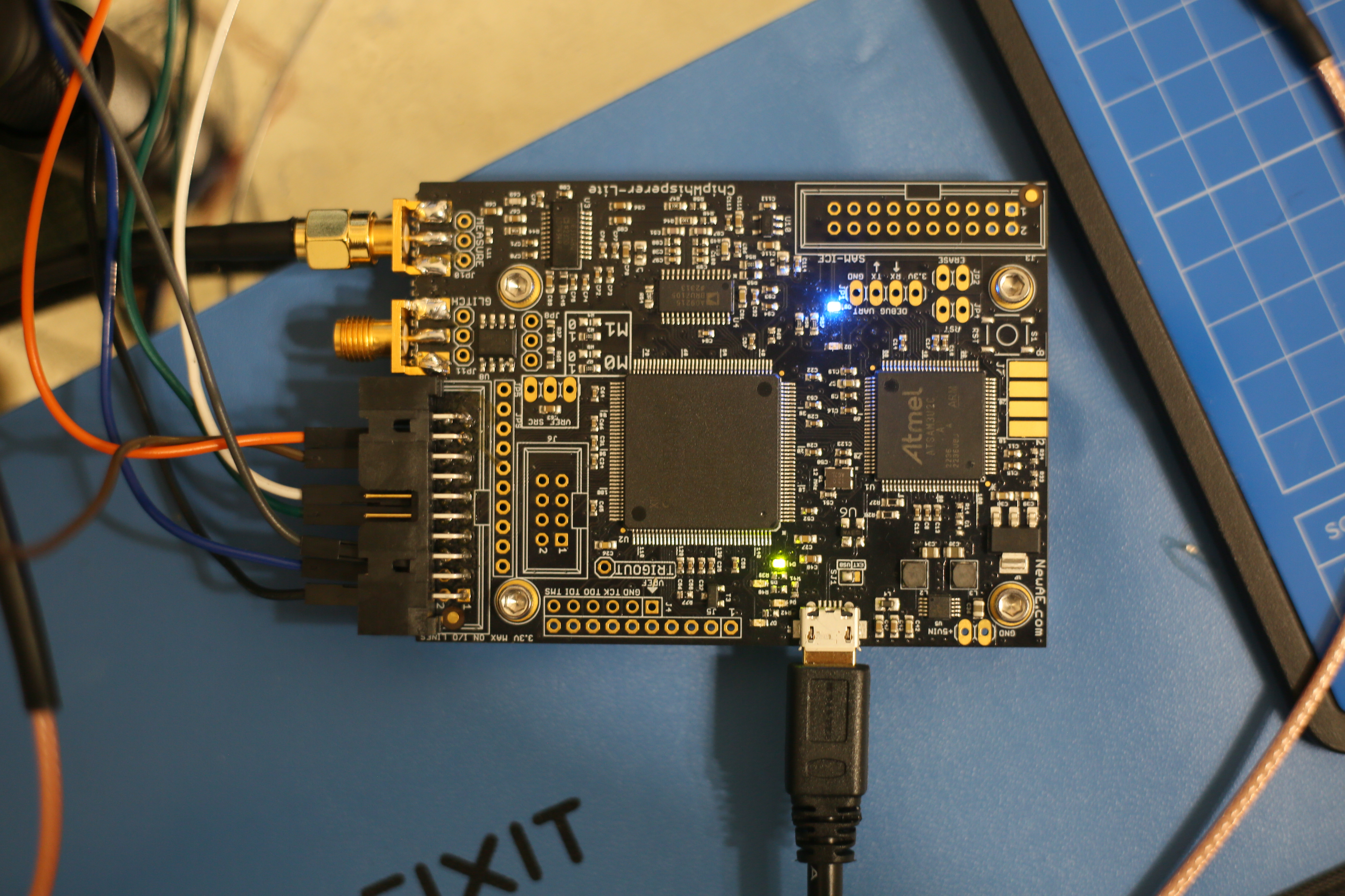
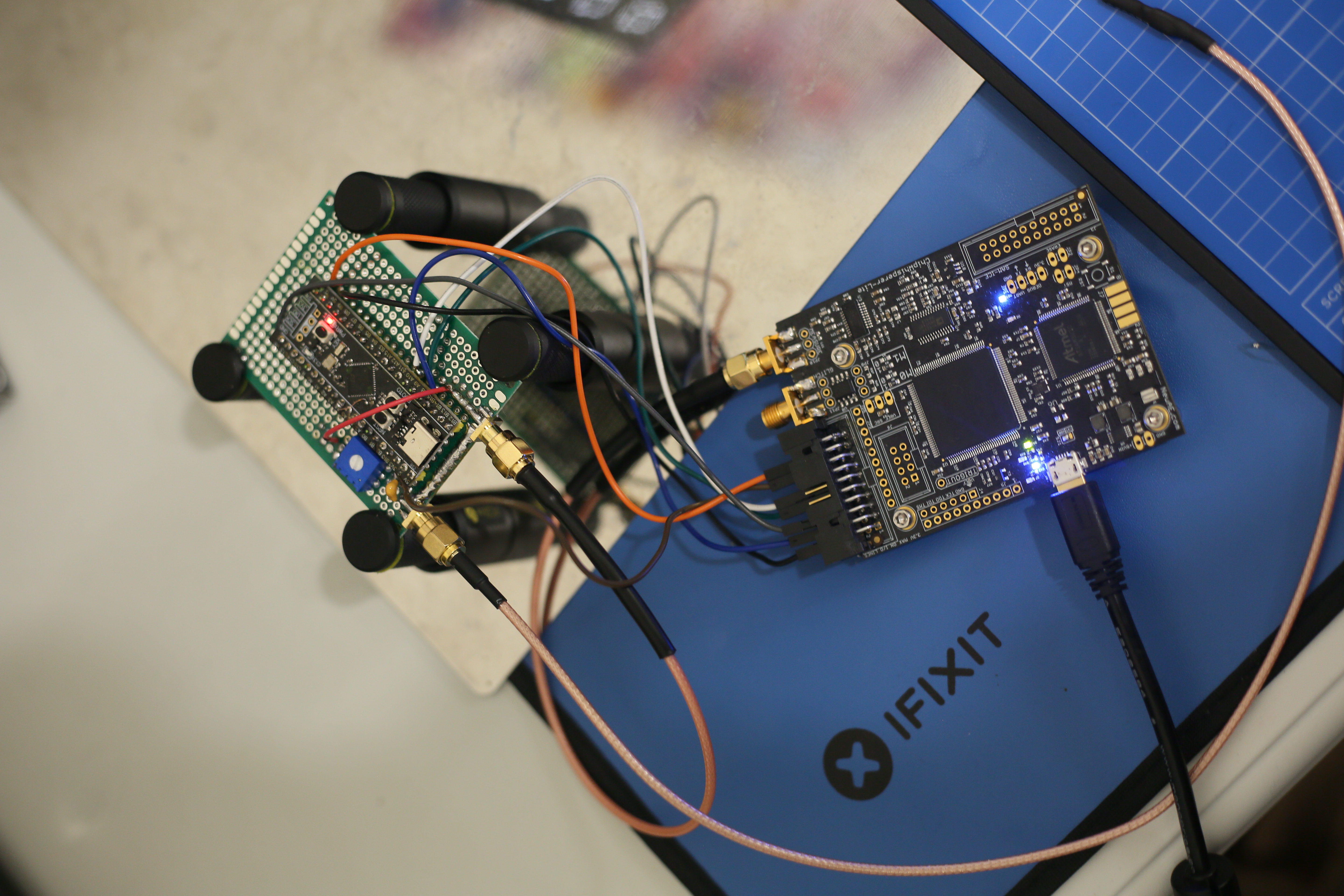
Gallery
Thank you to my camera man __kyson who took the photos for this post with his super duper top-of-the-line photo taking equipment. Listed here are some cool setup photos that could not have been fit anywhere else.

References
- Bedri Zija - Breaking Hardware AES on the MSPM0G3507: From Zero to Key
- Quarkslab - Bypassing Debug Password Protection on the RH850 Family Using Fault Injection
- NewAE Technology - Targets with Internal Regulators
- NewAE Technology - CW308T STM32F Target
- NewAE Technology - CW308T STM32F Socket Target
- NewAE Technology - UFO Target Boards
- NewAE Forum - CW308T STM32F4 Weird Spikes in Power Trace
- NewAE Forum - Necessity of Shunt Resistors
- STMicroelectronics - STM32F401xC Datasheet
- WeAct Studio - STM32F401CEU6 Black Pill V3.0 Schematic
- WeAct Studio - MiniSTM32F4x1 GitHub Repository
- STM32-base - WeAct Black Pill V3.0 Board Reference
- Colin O’Flynn, Jasper van Woudenberg - The Hardware Hacking Handbook
- Travis Goodspeed - Microcontroller Exploits
- LiveOverflow - RSA Power Analysis Side-Channel Attack - rhme2
- elbee - My Jupyter Notebook for this Target